Heterogenous Packaging
Terms
Wafer: Used as base die, can be active die (with transistors) or just passive (metal routing only) – if passive it is called a Si interposer.
Chiplet/die: a diced wafer – these are placed on either an active or passive base.
D2P - die-to-package: any signal exposed at the package substrate ball.
D2D - die-to-die: any interface between die not exposed at the package substrate ball.
TSV - Through-silicon-vias: exist on base die (active or passive) to route signals from top die/chiplets to bottom of package (creates D2P signal from top die/chiplets).
Die Mounting Options
Wafer on Wafer – Typically used for mature high-yield products/processes.
Bonded wafers diced into individual “stacked” die after wafer mounting.
Pro: Simpler process, less ESD risks, typically no D2D ESD risk after wafer bonding
![]()
Con: Only wafer sort testing can be completed – less coverage, mature
Chiplet on Wafer – Can be one or more chiplets on one base die.
Base wafer diced after chiplets are mounted on base die.
Pro: Functional testing of the top chiplets can be completed to screen out bad die before mounting. Can put many chiplets on one base die.
![]()
Con: More complex process introducing more ESD risks
Configurations
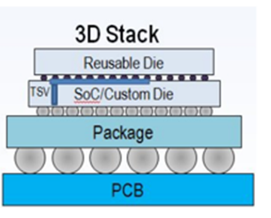
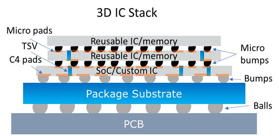
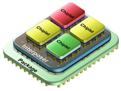
Die/Chiplets are then mounted on a package.
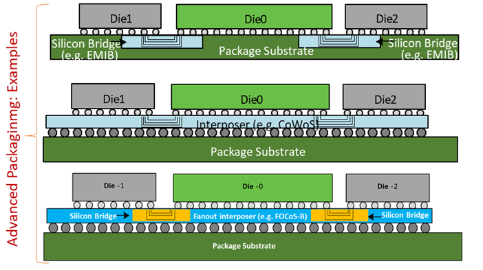
Communication between layers occurs through bumps, micro bumps, through-silicon vias (TSV), direct die-to-die connections, and silicon bridges (EMIBs).
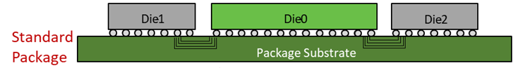
2D – multichip package with D2D interface through package substrate
2.5D – multichip package with D2D interface through silicon interposer, silicon bridge, fanout interposer, etc.
3D – multichip package with D2D interface through 2 active die
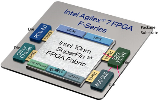
Examples of 2.5D and 3D products – note the Intel product is using both 3D and 2.5D configurations: (Fabric chip is 3D with 2.5D configuration through EMIB)
Problem Statements:
- Micro bump pitch: Today it is typically 25µm to 110µm pitch – hybrid bonding techniques will push this to below 10 µm.
- How do companies test bare die bumps and micro bumps for ESD robustness (CDM)? (The CDM JWG is discussing this)
- Not exposed at the package level
- There are no commercially available testers on the market.
- Can probe 25 to 110µm pitch bumps. New hybrid micro bumps are too small to probe with even TLP probes. Commercial CDM testers cannot test even the 25 to 110µm pitch - typically best they can do is 0.3mm.
- The number if micro bumps can vary from hundreds to 30,000+ bumps – these cannot all be tested.
- There is no qualification test, so believe people are currently using some form of TLP (vf-TLP or cc-TLP) to convince themselves that it meets a theoretical level.
- Only other alternative is to put the die (top or base)/chiplet in a “debug” package and test the package for CDM the traditional way. Since die/chiplet was not intended to go into a package – this is an expensive option.
- Manufacturing control – The risks in this are the tolls used to “handle” these wafers/die/chiplets – completed an ESD process assessment of each tool is needed to figure out how well things can be controlled and determine the level of CDM risk (WG 17 to address).
- EDA enablement/needs for chiplets - need to put ESD protection on the micro bump nets, this could be explicit ESD protection (diodes, etc.) or the interface could be “self-protected”. Both techniques are used today. Challenge: how do you complete the checks on a large quantity of interfaces? There may also be other challenges (WG 18 to address).