Dear ESDA Experts,
I’m currently working on a root cause investigation for an ESD burn mark issue on a semiconductor MCOB panel (IC product), and I would really appreciate some guidance or feedback from the community.
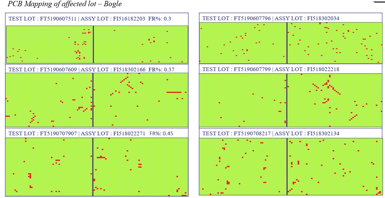
We observed a high reject rate across 6 lots, all showing similar failure patterns. Upon detailed panel strip mapping, one specific lot (attached example) revealed:
- A slanted/diagonal line pattern of failures on one strip.
- Clustered horizontal failure patterns on another section.
- Scattered failures throughout remaining areas.
Actions Taken So Far:
- Process-to-machine traceability mapping done for each lot.
- Strip failure mapping overlaid across lots to observe consistency.
- Fail rate mapping per machine revealed the issue likely started on April 5, 2025.
- Working hypothesis: issue may be ESD-related, with diagonal propagation path caused by process/equipment imbalance.
My Questions to the Forum:
-
In your experience, what could cause a consistent diagonal failure pattern in panel-level MCOB ESD defects, especially when process machines (Sawing, Sputtering, LM) operate orthogonally?
-
Is it plausible for ESD discharge paths to follow a diagonal route due to uneven grounding, ion imbalance, or warped tape tension?
-
What’s the best practice to validate ionizer coverage across an entire MCOB panel — especially at diagonal zones?
-
Have you seen cases where fixture trays or support beds cause partial grounding or act as unintentional ESD discharge points?
-
Would it make sense to perform a DOE-style re-run of a test lot across different suspect machines (e.g., SPTR, Detape, LM) to isolate a source?
Our Goal:
- To identify the actual ESD discharge point or failure trigger.
- To validate if ionizer direction, UV tape behavior, or mechanical fixture warping is the cause.
- To eliminate the possibility of false attribution to post-process handling or FAVI/OQA stations.
Any insights, best practices, or similar past case studies you can share would be incredibly helpful. Thank you!