# Thermoforming tray resistance
**URL:** https://forum.esda.org/t/thermoforming-tray-resistance/1505
**Category:** Uncategorized
**Created:** [October 5, 2026, 3:55pm UTC](https://forum.esda.org/t/thermoforming-tray-resistance/1505 "2026-10-05T15:55:24Z")
**Posts on this page:** 6
**Page:** 1
### Author:  [@SarbanR](https://forum.esda.org/u/SarbanR)
#### Post date: [October 5, 2026, 3:55pm UTC](https://forum.esda.org/t/thermoforming-tray-resistance/1505/1 "2026-10-05T15:55:24Z")
Hello Vijay Sir, Andy Sir & JK Sir,
I would like to confirm one point with you regarding the recently received thermoforming tray lot from the supplier.
The Point-to-Point resistance of the trays was measured in the range of 10^3 Ω, while the Point-to-Ground resistance was around 10^7 Ω as these trays are going to be used with trolley and workstation.
I rejected the lot considering 10^3 Ω as the lower limit. However, the supplier is requesting us to accept the trays, stating that there is no ESD risk with the 10^3 Ω resistance.
Could you please advise on this and confirm whether we can continue using trays with a Point-to-Point resistance of 10^3 Ω for PCBA handling and storage?
Thank you in advance.
---
### Author:  [@esdtekniks](https://forum.esda.org/u/esdtekniks)
#### Post date: [October 5, 2026, 8:48pm UTC](https://forum.esda.org/t/thermoforming-tray-resistance/1505/2 "2026-10-05T20:48:06Z")
Greeting of the day from India, to all the members on this forum.🌹
Rahul Sir,
I love to see your postings regularly as well as from others too on this forum which keeps energizing me to remain active and providing continuous opportunity to learn in this field even at 72.
Good question indeed .This is how we can understand the practical issues faced by real users who want to use the right EPEs with proper knowledge which is very much required in the ESD control -in the electronic sector at least in India. Because even after four and a half decades of this ESD concept in Indian electronic sector still in 90 percent of the industry it is just at the grass root level with total ignorance - negligence but the industries are easily getting the label ANSI ESD S 20 20 / IEC 61340-5-1 ESD FACILITY CERTIFIED. Till date I am unable to understand the value or concept behind of this facility certification when the basic compliance is not found okay in many places.
well; coming to your question with the little knowledge I have, I would like to put up my views as under and look forward to our ESDA experts and other colleagues comments as well soon.
1. What was the technical condition of your purchase order ?
2. Was the sensitivity of your device you were to place inside the said EPE considered prior
to deciding the said EPE and is not meeting your requirements ?
3. Did the supplier supply you the said EPE with a detailed PQ test report per the applicable
test methods **or** did you get the PQ test report within facility **or** got done from a
third party before putting into use ?
It is mandatory for the packaging items that it shall undergo PQ tests at 12%+/- 3 as
well as at 50+/-5 % at temperature 23+/- Degree C prior to its use .
4. What was the ambient condition at your EPA when you checked the said EPEs ?
5. In general the P-P tests and Point to ground able point (Rtgp)resistance both are
required during the PQ test and for the compliance test it is only the point to ground
resistance which is the **most critical parameter** to confirm the item’s ability to
safely conduct an electrostatic charge away from the surface to the EPA’s grounding
system.
6.Considering the CDM Risk, P-P e3 ohms range will be highly conductive per the ANSI/
ESD S541 as the packaging materials that comes into intimate contact with the sensitive
component be ideally be in dissipative range \> 1 x e4 to \<1 x e11 ohms .
7.Since your observations are perhaps in the ambient conditions , compliance verification
point of view I do not foresee anything wrong in accepting the said items provided that
the components or devices you are placing inside these trays are normal EDS-sensitive
items but not very highly sensitive components in CDM limits and you do not experience
the same e3 ohms P-P through out,
6. In case you continue to experience the same e3 ohms at lesser Rh% anytime in between
and if you happen to place highly sensitive components in CDM limits then perhaps you
will have no option except to reject the items under subject discussion.
7. However, in my opinion it is better you get a detailed PQ test report from a certified lab
per the applicable test methods per ANSI ESD S541.
8. Because it is showing P-P e3 and Rtg e7 I doubt about the said EPEs homogeneous
property and perhaps it is not ESD safe volume resistance wise and the surface could
be a conductive spray coated .
Look forward to experts comments and your comments as well .
Thank you
---
### Author:  [@SarbanR](https://forum.esda.org/u/SarbanR)
#### Post date: [October 6, 2026, 5:34am UTC](https://forum.esda.org/t/thermoforming-tray-resistance/1505/3 "2026-10-06T05:34:10Z")
Hello Mr. Vijay Sir,
Thank you so much for your prompt response.
These conductive trays are qualified as per the product qualification requirements at 12% ±3% RH as well as 50% ±5% RH. Currently, these trays are being used in an environment with 40% to 60% RH.
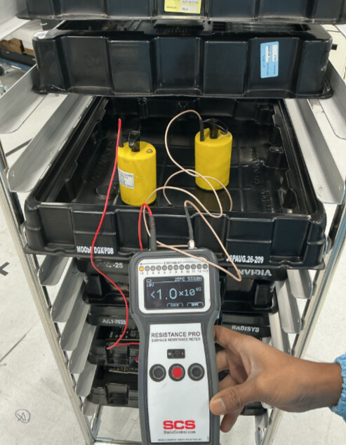
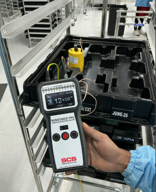
We are using these trays on a movable trolley, as shown in the attached picture.
So, could you please review the above conditions and advise whether a 10^3 ohms tray would be suitable for this application?
Thank you for your support and guidance.
---
### Author:  [@esdtekniks](https://forum.esda.org/u/esdtekniks)
#### Post date: [October 6, 2026, 7:13am UTC](https://forum.esda.org/t/thermoforming-tray-resistance/1505/4 "2026-10-06T07:13:53Z")
Greetings of the from India, to all the members on this forum 🌹
Rahul Sir,
Thank you for your immediate feedback.
Thank you for sharing the images.
1. What is the conclusion result in the PQ report ? As ES conductive tray or ES dissipative tray ?
2. What was ordered by you ? As ES conductive tray or ES dissipative tray ?
3. What were the observed parameters at 12% +/- 3 Rh ?
4. Your image on P-P test shows that one of the probes is slightly lifted up and not
making perfect flat contact with the entire area to cover the base of the probe.
Could you please get it checked again?
5. Further , both the trays looks to be different and looks to the two measurements
are different and made on different trays .
6. Is the test per STM 11.12 done for volume resistance check ?
I feel doubt about its homogeneous property as the Rtg is higher to P-P.
7. In case you continue to experience the same e3 ohms or less at 40-60% Rh only or
at lesser Rh% anytime in between and if you happen to place highly sensitive
components in CDM limits, then perhaps you will have no option except to reject
the items under subject discussion provided you had specified you requirement in
the purchase order.
8. **However, if you can pack your PCBAs inside the static shielding bags and then
keep the enclosed packets inside the tray , it would be safe and good and no
issue in using the trays . Further it provides the required Faraday cage protection
also.**
Anyway let me have your feed back again and meanwhile let us welcome our experts and colleague members opinion also.
Thank You & good day 🌹
---
### Author:  [@AndyN](https://forum.esda.org/u/AndyN)
#### Post date: [October 6, 2026, 10:27pm UTC](https://forum.esda.org/t/thermoforming-tray-resistance/1505/5 "2026-10-06T22:27:02Z")
Rahul,
Many companies use conductive totes and even worksurfaces successfully because they are able to control the charging of the ESD sensitive components. Remember the limits in ANSI/ESD S20.20 for worksurfaces, shelving, and mobile carts are \< 10^9 ohms. There is no lower limit. There is a footnote that if CDM is a concern, you should consider setting a lower limit of 10^6 ohms, but even this may or may not be enough to prevent a CDM discharge if your ESD sensitive items have very low CDM limits and if there is no way to control charging. If you are placing the trays on a grounded cart, the ESD sensitive PCBAs are grounded when moving them into the trays, and the operators are grounded, then there is likely a low risk of a CDM discharge into the trays. If for some reason you are dealing with a very sensitive ESD item and you can’t be sure of it being grounded, you may need to move to a dissipative tray.
---
### Author:  [@SarbanR](https://forum.esda.org/u/SarbanR)
#### Post date: [October 7, 2026, 4:18am UTC](https://forum.esda.org/t/thermoforming-tray-resistance/1505/6 "2026-10-07T04:18:40Z")
Thank you so much Andy Sir for your more clarity and guidance on the CDM risk.